 +86 18902444860
 myd@merryoung.com


 French
 English
 Chinese
 Spanish
 Russian
 Italian
 German
 Japanese
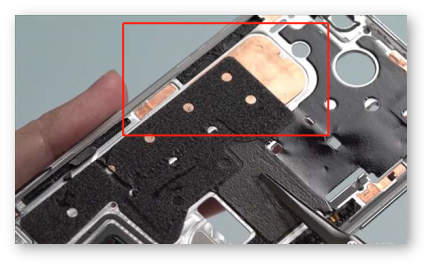
Dans les emballages semi-conducteurs, lecadre plombjoue un rôle crucial dans la connexion de la puce à des circuits externes. À mesure que les dispositifs électroniques deviennent plus petits et plus puissants, la précision de fabrication requise pour les cadres en plomb continue d'augmenter.
Aujourd'hui, les cadres en plomb sont généralement fabriqués en utilisantprocessus d'estampage ou de gravure chimiqueParmi ces méthodes, la gravure chimique est devenue de plus en plus importante en raison de sa capacité à produire des microstructures de haute précision.
Cet article explique legravure de cadre au plombprocessus et étapes clés de fabrication.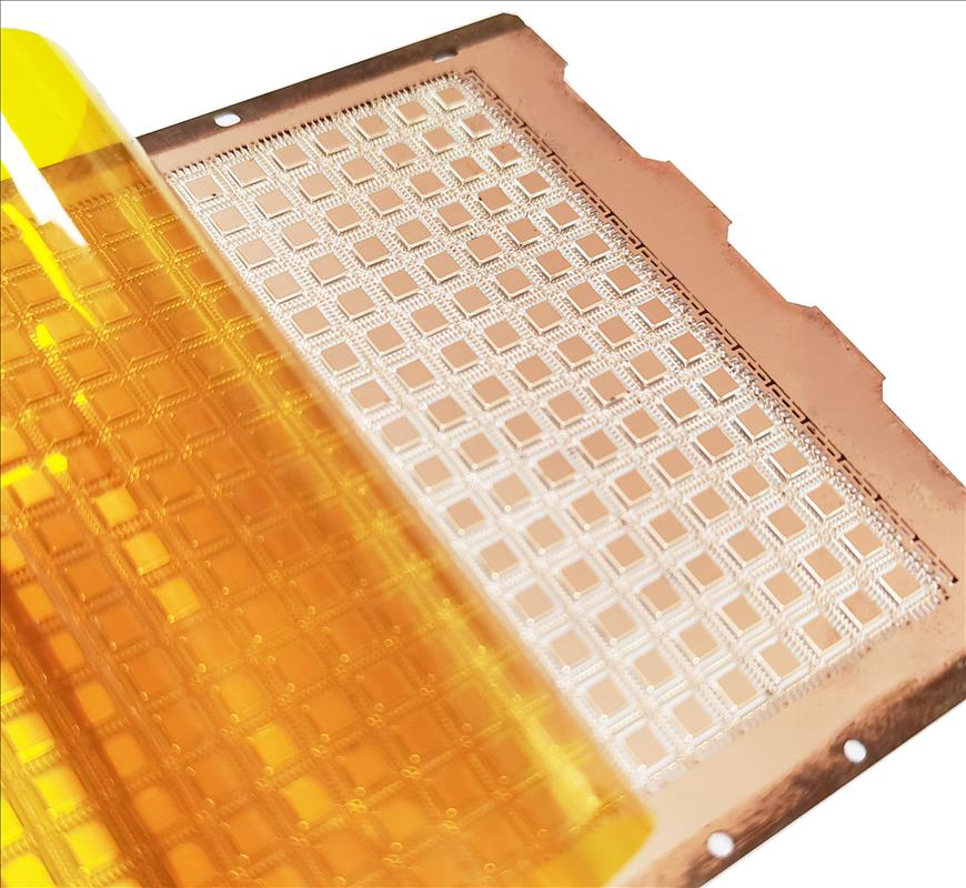
Les cadres en plomb sont généralement fabriqués de:
cuivre
Alliages de cuivre
Acier inoxydable
Ces matériaux sont généralement fournis entôles ou bobines métalliquespour la production.
Avant la gravure, acouche photorésistanteest appliqué sur la surface métallique.
Les étapes comprennent :
Nettoyage de surface
Revêtement photorésistant
Processus de séchage
Le photorésist agit comme couche protectrice pendant le processus de gravure.
En utilisant la technologie de photolithographie, le motif du cadre de plomb est transféré sur la surface métallique.
Cette étape comprend :
Alignement du masque
Exposition aux UV
Développement du modèle
Après cette étape, la surface métallique contient le schéma de circuit précis.
Gravure chimiqueest l'étape centrale du processus de fabrication du cadre de plomb.
Lors de la gravure, les zones métalliques exposées sont dissoutes parproduits chimiques de gravure pulvérisés sur la surface métallique.
Les avantages incluent :
Traitement de haute précision
Fabrication de micro-motifs
Qualité de gravure uniforme
Après la gravure, le photorésist restant est retiré.
Les processus comprennent :
Découpage photorésistant
Nettoyage de surface
Séchage
Cela garantit que la surface du cadre de plomb répond aux exigences d'emballage des semi-conducteurs.
L'étape finale comprend l'inspection du produit:
Inspection de précision dimensionnelle
Inspection de la qualité de la surface
Inspection de l'intégrité structurelle
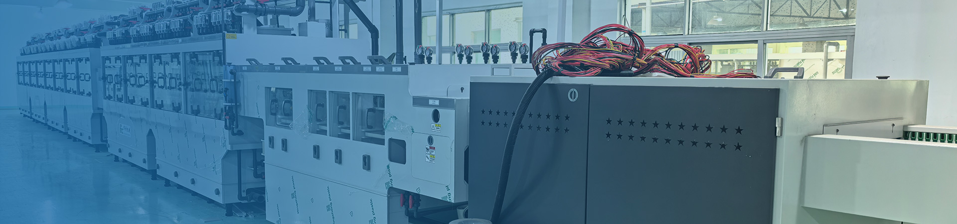
Dongguan Huazhou Machinery Technology Co., Ltd.spécialisé dans le développement et la fabrication deéquipement de gravure chimique métallique de précision.
Notre équipement est largement utilisé dans des industries telles que:
Cadres à plomb semi-conducteurs
Composants électroniques de précision
Écrans de filtration métallique
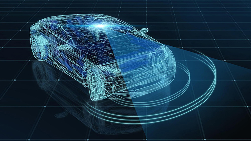
Pièces électroniques automobiles
Plaques bipolaires à pile à combustible à hydrogène
Système de gravure par pulvérisation de haute précision
La technologie avancée de gravure par pulvérisation assure une performance de gravure uniforme et une précision de traitement élevée.
Lignes de production automatisées
Nos systèmes soutiennent la production automatisée continue, améliorant l'efficacité de la fabrication.
Capacité de traitement multi-matériaux
Huazhouéquipement de gravurepeut traiter divers métaux, y compris:
cuivre
Acier inoxydable
aluminium
Alliages de nickel
Technologie respectueuse de l'environnement
Nos équipements sont conçus avec des systèmes chimiques optimisés pour réduire l'impact environnemental et améliorer la durabilité.
Dernières connaissances de gravure
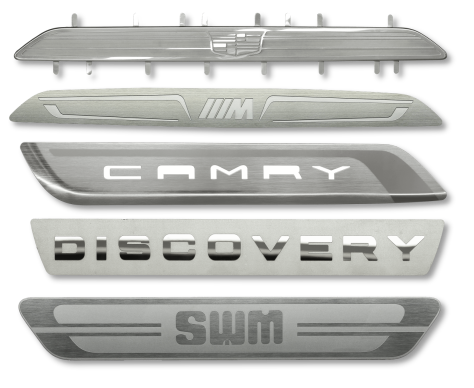
With the continuous upgrade of automotive consumption, customers are placing increasingly higher demands on vehicle interior design, quality, and craftsmanship.Automotive decorative trims — whether ap……
Related topics: Automotive Metal Etching SolutionIn the era of smart vehicles, in-car audio experience has become an important factor in evaluating vehicle luxury, comfort, and overall quality. As a c……
With the rapid advancement of 5G communications, smart devices, new energy vehicles, and high-performance computing platforms, the power consumption and heat generation of electronic equipment continu……
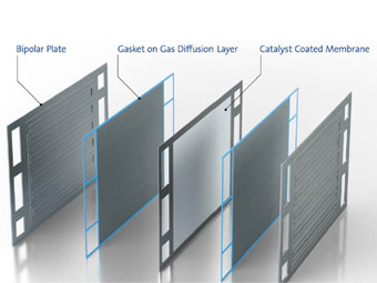
Avec le développement rapide de l'industrie des véhicules à énergie à hydrogène, les plaques bipolaires métalliques sont devenues l'un des composants de base les plus critiques des piles à com……
Envoyer une demande
Choisissez Huazhou Machinery pour protéger votre réputation.
Navigation rapide
Company
Contact Us
 No.1 Niuling Road, arc commémoratif, Sukeng, ville de Changping, Dongguan
 86 1890244860
 myd@merryoung.com


Copyright © Dongguan Huazhou Machinery Technology Co., Ltd.carte du site 粤ICP备18133982号